Personal design study · May – Oct 2026
Battery-powered HiFi player
A battery-powered music player designed end to end: schematic, four-layer board, power path, firmware.
The brief
A battery-powered HiFi music player, started in May 2026 and designed end to end: schematic capture, a four-layer PCB layout, the power path, and firmware on an ESP32-S3R8.
I wanted one project that went through every step of a real product board rather than a dev kit with wires: choosing the parts, drawing the schematic, laying out a 4-layer board with a proper power path for a battery, and then writing the firmware that makes it play music. A music player is a good vehicle for this; it is obvious when it does not work.
Two sources, one DAC
Audio streams in from Bluetooth or from a microSD card. Either source is routed through a MUX into an I2S DAC (Fig. 1). The ESP32-S3R8 handles both sources on the same chip.
The board is four layers (Fig. 2). The power path is designed for battery operation, so the whole thing was meant to leave the bench.
The board
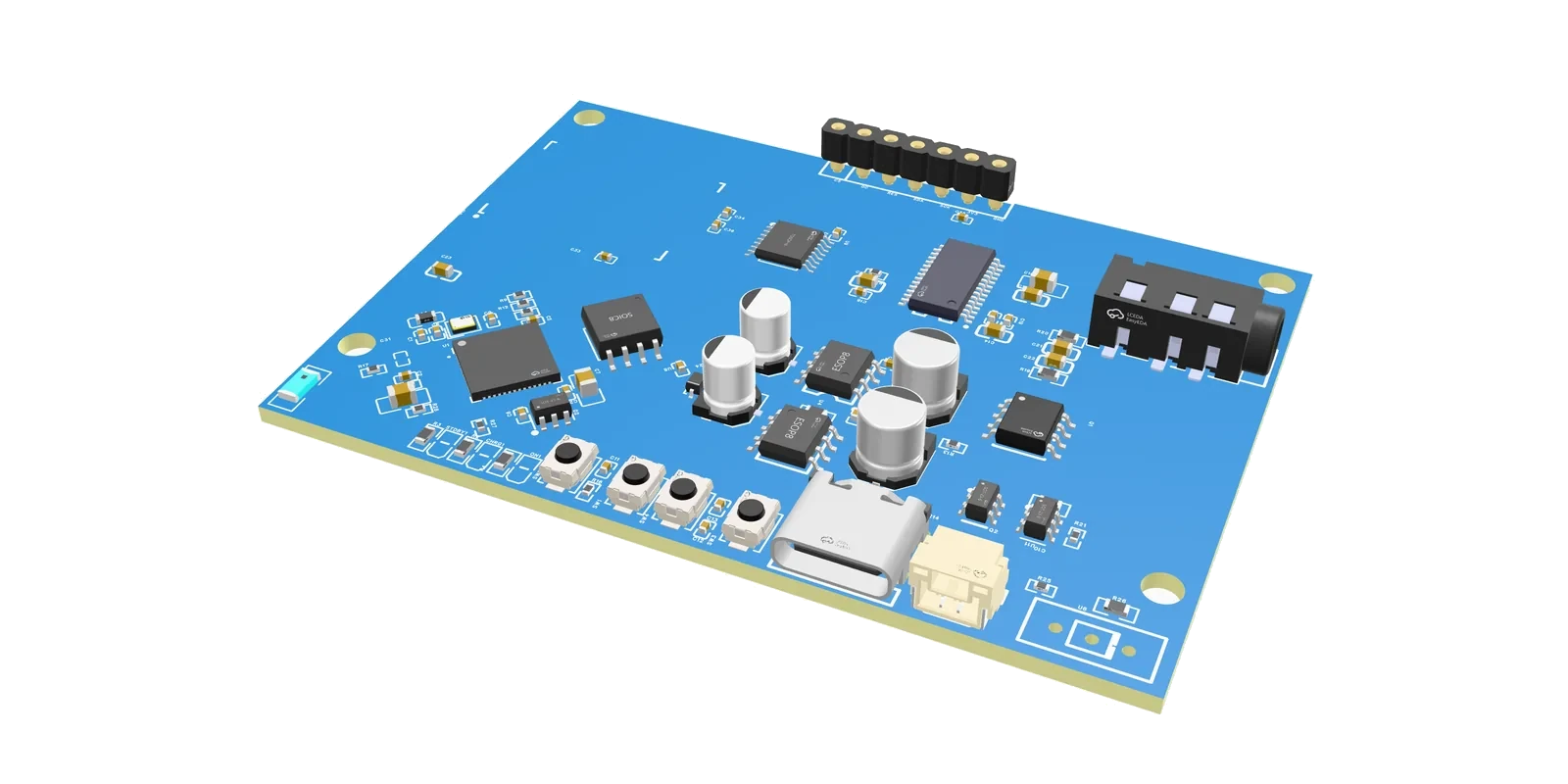
This is the current layout as a 3D model, straight from the EasyEDA Pro export: 70.9 × 50.4 mm, and 8.5 mm deep with the parts on. It is the design file, not a photograph; nothing on it was ever assembled.
Three revisions
The layout has been through three revisions. Revision 1 is a small board with two buttons, a USB-C connector, a 3.5 mm jack, a large rotary control and a 4-pin header.
Revision 2 is a larger board that adds a Bluetooth module with its own crystal, four buttons, a microSD slot and the ESP32-S3R8 with its crystal.
Revision 3 has four mounting holes, with the module and the ESP32 on the left, the DAC section and the 3.5 mm jack top right, two electrolytic capacitors and the power section in the middle, USB-C, microSD and a JST battery connector along the bottom edge, and a 7-pin screen header at the top.
Where it stopped
I stopped the project in October 2026 at the design stage, to put the time into a project I find more engaging. It stands as a design exercise without physical verification: the schematic and the layout are done, and nothing was assembled, powered or tested, so nothing on this page is a measured result.
- doneschematic capture
- done4-layer PCB layout (three revisions)
- not builtpower path bring-up
- not finishedESP32-S3R8 firmware
- not builtboard bring-up
The layout exists in three revisions. No board was assembled or powered, so there are no photographs of a built board.